- 您现在的位置:买卖IC网 > Sheet目录1242 > SFPA32GBQ1BO8TO-I-QT-223-STD (Swissbit NA Inc)FLASH SSD SMART UDMA 2.5" 32GB
�� �
�
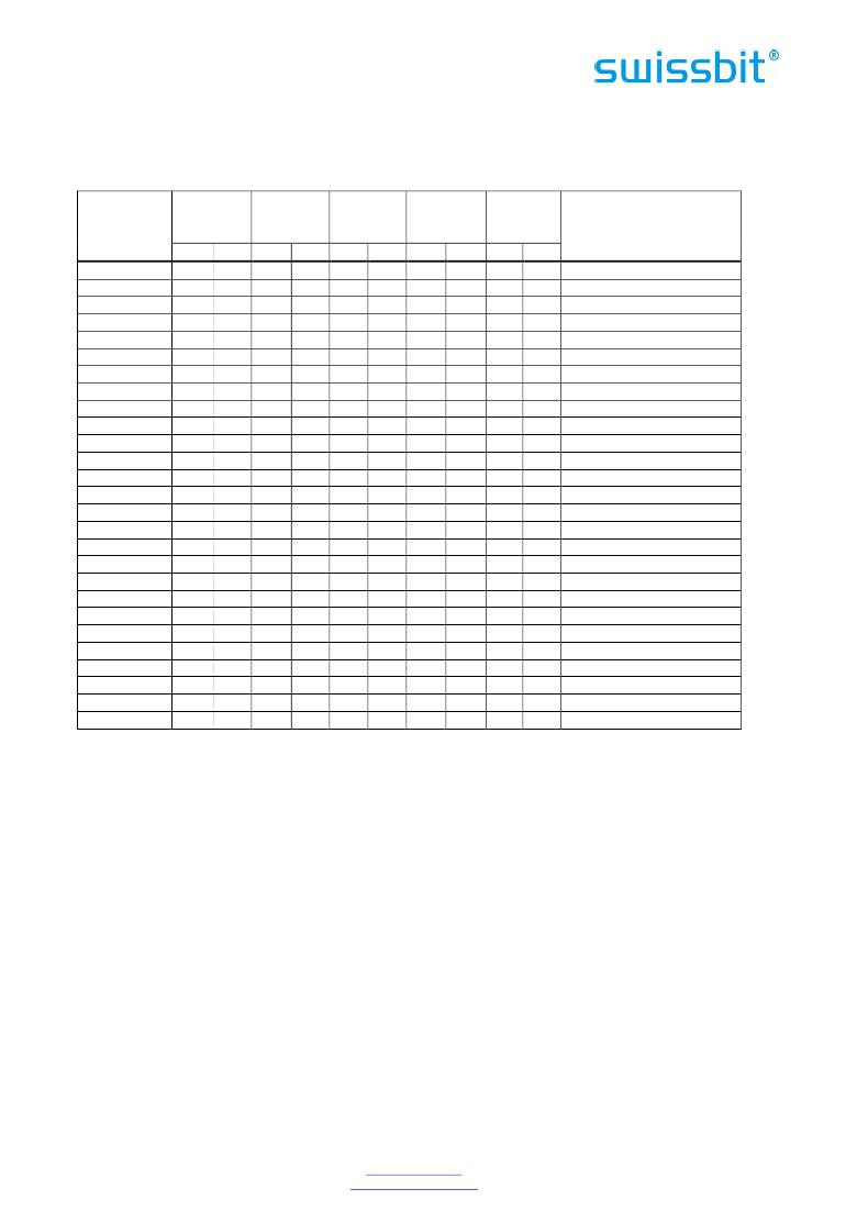
�6.3.2.4� Ultra� DMA� Data� Transfers� Timing�
�Table� 22� and� Table� 23� define� the� timings� associated� with� all� phases� of� Ultra� DMA� bursts.�
�Table 22: Ultra� DMA� Data� Burst� Timing� Requirements�
�Name�
�UDMA�
�Mode� 0�
�(ns)�
�UDMA�
�Mode� 1�
�(ns)�
�UDMA�
�Mode� 2�
�(ns)�
�UDMA�
�Mode� 3�
�(ns)�
�UDMA�
�Mode� 4�
�(ns)�
�Measurement� location�
�(See� Note� 2)�
�Min�
�Max� Min� Max� Min� Max� Min�
�Max� Min� Max�
�t� 2CYCTYP�
�t� CYC�
�t� 2CYC�
�t� DS�
�t� DH�
�t� DVS�
�t� DVH�
�t� CS�
�t� CH�
�t� CVS�
�t� CVH�
�t� ZFS�
�t� DZFS�
�t� FS�
�240�
�112�
�230�
�15.0�
�5.0�
�70.0�
�6.2�
�15.0�
�5.0�
�70.0�
�6.2�
�0�
�70.0�
�230�
�160�
�73�
�153�
�10.0�
�5.0�
�48.0�
�6.2�
�10.0�
�5.0�
�48.0�
�6.2�
�0�
�48.0�
�200�
�120�
�54�
�115�
�7.0�
�5.0�
�31.0�
�6.2�
�7.0�
�5.0�
�31.0�
�6.2�
�0�
�31.0�
�170�
�90�
�39�
�86�
�7.0�
�5.0�
�20.0�
�6.2�
�7.0�
�5.0�
�20.0�
�6.2�
�0�
�20.0�
�130�
�60�
�25�
�57�
�5.0�
�5.0�
�6.7�
�6.2�
�5.0�
�5.0�
�6.7�
�6.2�
�0�
�6.7�
�120�
�Sender�
�Note� 3�
�Sender�
�Recipient�
�Recipient�
�Sender�
�Sender�
�Device�
�Device�
�Host�
�Host�
�Device�
�Sender�
�Device�
�t� LI�
�0�
�150�
�0�
�150�
�0�
�150�
�0�
�100�
�0�
�100�
�Note� 4�
�t� MLI�
�t� UI�
�t� AZ�
�t� ZAH�
�t� ZAD�
�20�
�0�
�20�
�0�
�10�
�20�
�0�
�20�
�0�
�10�
�20�
�0�
�20�
�0�
�10�
�20�
�0�
�20�
�0�
�10�
�20�
�0�
�20�
�0�
�10�
�Host�
�Host�
�Note� 5�
�Host�
�Device�
�t� ENV�
�20�
�70�
�20�
�70�
�20�
�70�
�20�
�55�
�20�
�55�
�Host�
�t� RFS�
�t� RP�
�t� IORDYZ�
�t� ZIORDY�
�t� ACK�
�t� SS�
�160�
�0�
�20�
�50�
�75�
�20�
�125�
�0�
�20�
�50�
�70�
�20�
�100�
�0�
�20�
�50�
�60�
�20�
�100�
�0�
�20�
�50�
�60�
�20�
�100�
�0�
�20�
�50�
�60�
�20�
�Sender�
�Recipient�
�Device�
�Device�
�Host�
�Sender�
�Notes:�
�1.�
�2.�
�3.�
�4.�
�5.�
�6.�
�All� timing� measurement� switching� points� (low� to� high� and� high� to� low)� shall� be� taken� at� 1.5� V.�
�All� signal� transitions� for� a� timing� parameter� shall� be� measured� at� the� connector� specified� in� the�
�measurement� location� column.� For� example,� in� the� case� of� tRFS,� both� STROBE� and� –� DMARDY�
�transitions� are� measured� at� the� sender� connector.�
�The� parameter� tCYC� shall� be� measured� at� the� recipient’s� connector� farthest� from� the� sender.�
�The� parameter� tLI� shall� be� measured� at� the� connector� of� the� sender� or� recipient� that� is� responding�
�to� an� incoming� transition� from� the� recipient� or� sender� respectively.� Both� the� incoming� signal� and�
�the� outgoing� response� shall� be� measured� at� the� same� connector.�
�The� parameter� tAZ� shall� be� measured� at� the� connector� of� the� sender� or� recipient� that� is� driving� the�
�bus� but� must� release� the� bus� the� allow� for� a� bus� turnaround.�
��Swissbit� AG�
�Industriestrasse� 4�
�Swissbit� reserves� the� right� to� change� products� or� specifications� without� notice.�
�Revision:� 1.00�
�CH-9552� Bronschhofen�
�Switzerland�
�www.swissbit.com�
�industrial@swissbit.com�
�P-120_data_sheet_PA-QxBO_Rev100.doc�
�Page� 17� of� 76�
�发布紧急采购,3分钟左右您将得到回复。
相关PDF资料
SFPK-SL
CONN SFP CAGE
SFSA16GBV1BR4TO-I-QT-226-STD
FLASH SLC UDMA/MDMA/PIO 16GB
SFSA32GBQ1BR8TO-I-QT-226-STD
FLASH SLC UDMA/MDMA/PIO 32GB
SFSA32GBU1BR4TO-I-NC-216-STD
FLASH X-200M SLC MSATA 32GB
SFSA32GBV1BR4TO-I-NC-216-STD
FLASH X-200S SLC SLIM SATA 32GB
SFSA64GBQ1BR8TO-I-NC-216-STD
FLASH SSD UDMA IND 2.5" 64GB
SFSO4404NR
FEMALE SCREWLOCK 4-40 .197"
SFW22R-1STE1
SFW22R-1STE1-FFC/FPC CONN
相关代理商/技术参数
SFPA32GBQ1BO8TO-I-QT-243-STD
制造商:SWISSBIT NA INC 功能描述:FLASH
SFPA36AT0250
制造商:General Electric Company 功能描述:SFP 3P 600V 250A
SFPA4096Q1BO2TO-C-DT-243-STD
制造商:SWISSBIT NA INC 功能描述:FLASH
SFPA4096Q1BO2TO-I-DT-223-STD
功能描述:FLASH SSD SMART UDMA 2.5" 4GB RoHS:是 类别:计算机,办公室 - 元件,配件 >> 固态硬盘驱动器 系列:P-120 标准包装:1 系列:- 存储容量:64GB 存储器类型:闪存 - NAND 其它名称:VL 64 GB SSHD KITVL64GBSSHDKIT
SFPA4096Q1BO2TO-I-DT-243-STD
制造商:SWISSBIT NA INC 功能描述:FLASH
SFPA-53
制造商:未知厂家 制造商全称:未知厂家 功能描述:Schottky Barrier Diodes
SFPA-63
制造商:SANKEN 制造商全称:Sanken electric 功能描述:Schottky Barrier Diodes (Surface Mount) 30V
SFPA-73
制造商:未知厂家 制造商全称:未知厂家 功能描述:Schottky Barrier Diodes